

Your first board check
This is a real board with real problems. Not a toy: an Arduino UNO shield with an RGB LED, a resistor, a tactile switch and four mounting holes. It has five errors on the PCB, two on the schematic, and several mistakes that no KiCad check will ever report — which turn out to be the most interesting things in it.
You will need KiCad 9 or newer, and about twenty minutes. KiCad does not need to be running — everything here reads the files.
Get the project
Section titled “Get the project”Download Copperplane_Blink_LEDs.zip
— about 35 KB, three files. Unzip it anywhere and open the .kicad_pro in KiCad.
(The same files live in
examples/Copperplane_Blink_LEDs/
if you would rather browse them or already have the repository.)
Look at the schematic and the board for a minute before Copperplane sees them — it is worth having your own impression to compare against.
Link it
Section titled “Link it”In Copperplane, make a new project and point it at the .kicad_pro file.
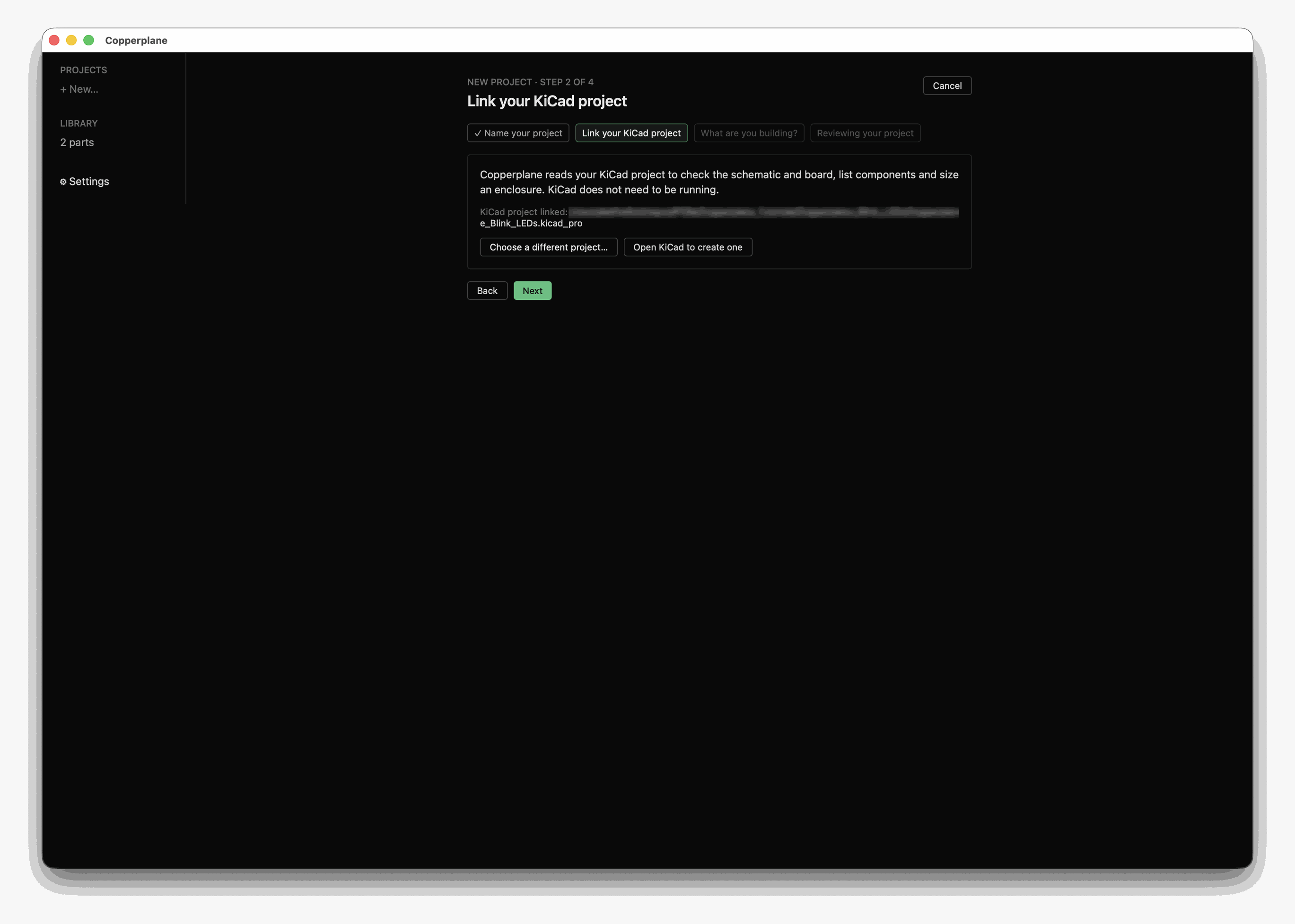
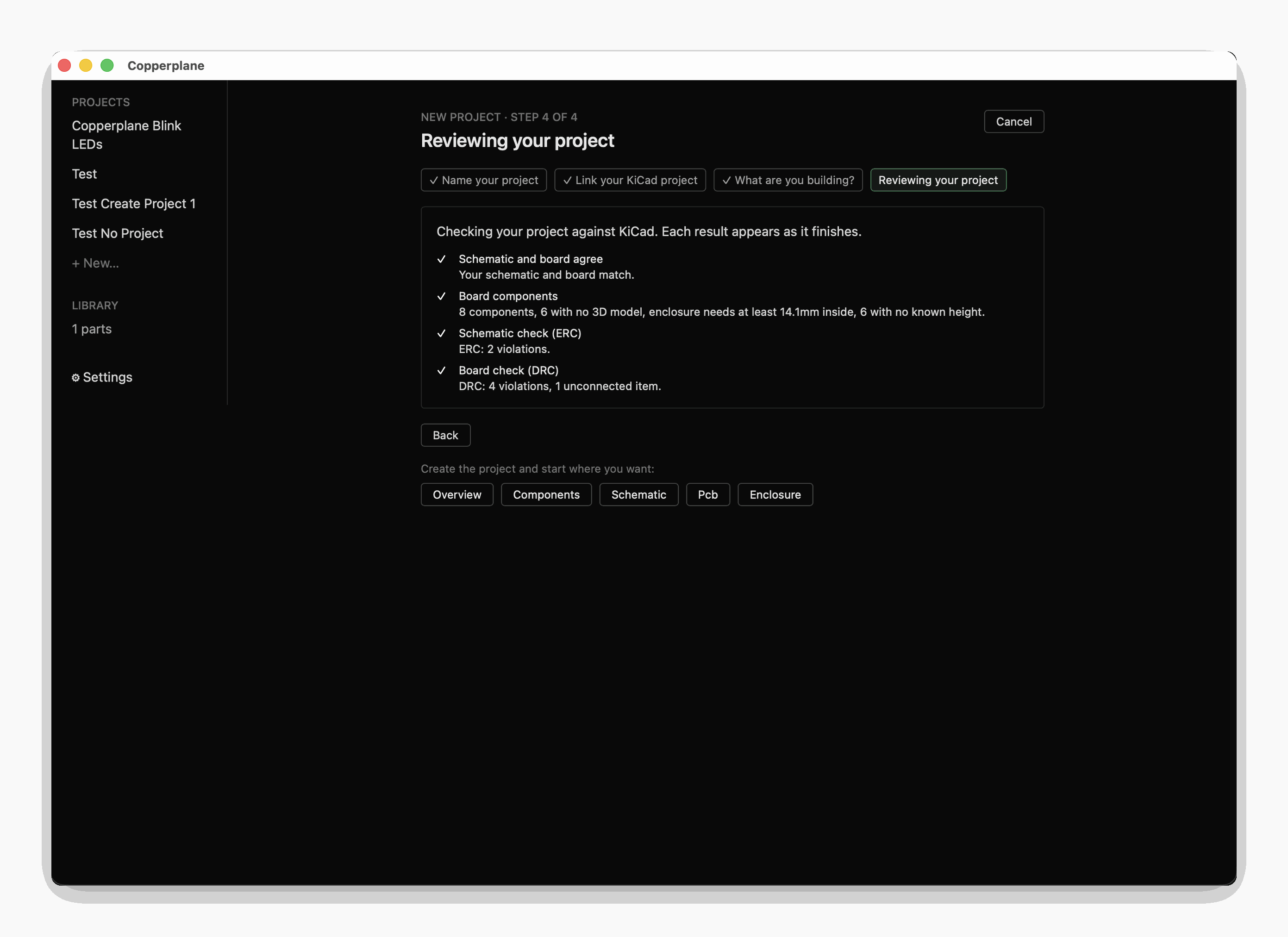
The last step of the wizard checks the project as it links it — schematic and board agreeing, the component count, and what ERC and DRC already have to say. You have not asked for anything yet and it has already read the design.
The rail on the left holds your projects, your parts library, and Settings. Across the top of a project sit five tabs — Overview, Components, Schematic, PCB, Enclosure — which is roughly the order you would work in.
What it says before you ask
Section titled “What it says before you ask”Stay on Overview. You have run no check and asked no question, and it already has three things to say about this board.
One is a blocker dressed as a detail.
R1 still has KiCad’s placeholder value (R). Until it says what it actually is, nothing here can work out what this circuit draws — and that is what a trace width and a power budget both rest on.
R is what KiCad puts there when you place a resistor and never come back. It is
not an error to KiCad — the part is perfectly well-formed — but it is the reason
several other questions about this board cannot be answered at all. Notice that
the app says which questions rather than just complaining.
One is the sort of thing you find with a multimeter, three hours in.
A1 pin 8 is its VIN pin, and you have the +5V rail on it. This part also declares a 5V output pin of its own, which means VIN is the input that feeds whatever makes that — so the two are not interchangeable. Its own 5V pin (pin 5) is not connected to anything.
VIN on an Arduino goes through the board’s own regulator. Feeding it a
regulated 5V leaves that regulator nothing to work with, and the 5V rail it
produces comes out lower than 5V. The pin that actually is 5V — pin 5 — is
sitting unconnected right next to it.
Note the last sentence of that finding, which is a question rather than a verdict: is +5V what you meant here? The app cannot see inside the Arduino module. A different board might accept 5V on VIN quite happily, so it tells you what it can see and leaves the judgement with you.
And one is the board being right, which you would otherwise never hear about:
D1’s anode reaches R1 on Net-(D1-A) — that resistor is what stops the LED drawing more current than the pin driving it can give.
That is deliberate. A check that only ever speaks up when something is wrong teaches you nothing about the times you got it right, and “no findings” is indistinguishable from “nothing was looked at”. Each of these also names what was not examined, so a quiet Overview is never mistaken for a finished board.
None of the three is an ERC or DRC violation. Every one is read from your schematic’s actual connectivity — which pin joins which net — and every number in them comes from your files rather than from a model’s impression of your files.
Read the board
Section titled “Read the board”Open the Schematic tab.
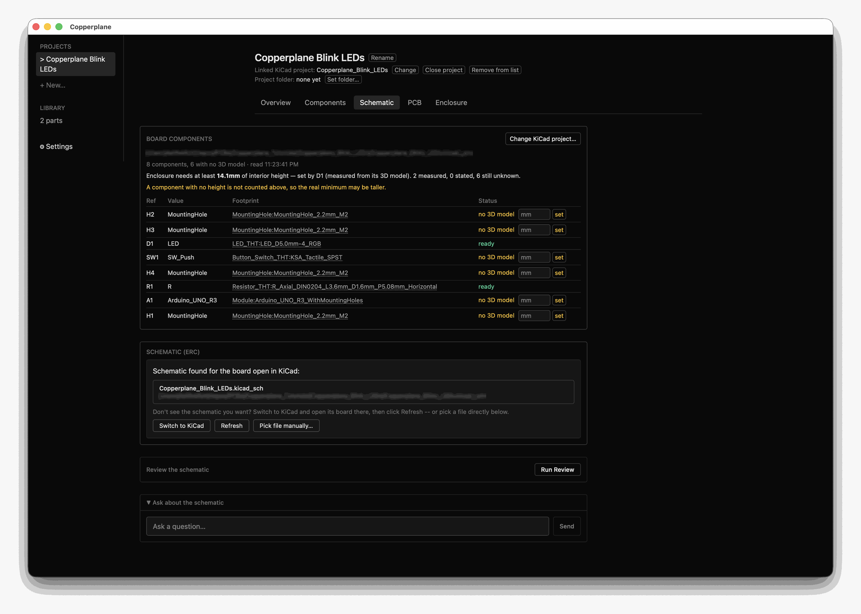
Eight components. Six of them have no 3D model, which is not an error — most KiCad footprints ship without one — but it matters later, and Copperplane says so rather than quietly assuming a height of zero.
Notice what it already knows: the enclosure needs at least 14.1 mm of interior height, and that figure comes from D1, measured from its 3D model. It also tells you the number is a floor rather than an answer, because six components could not be measured at all.
That is the shape of everything here. A number, where it came from, and what it does not cover.
Check the PCB
Section titled “Check the PCB”Open the PCB tab and run the check.
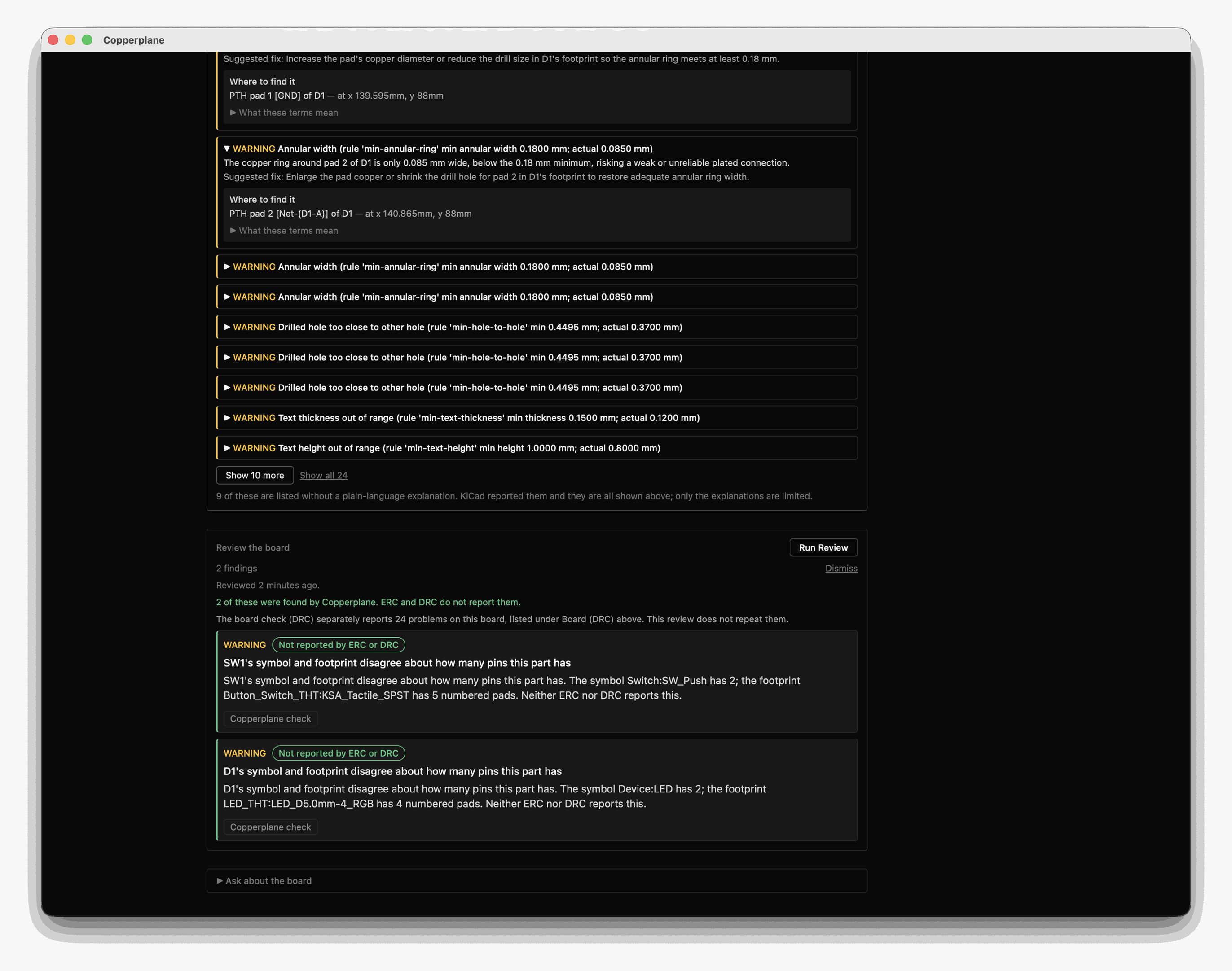
Five findings, from two different places. Three of them explain KiCad’s own DRC, which counts five violations here. The other two are Copperplane’s own, and KiCad reports neither of them at all.
Start with the three.
One — four pads, one problem. KiCad reports the same violation four times, once per pad of D1. It reads like this:
Annular width (board setup constraints min annular width 0.1000 mm; actual 0.0850 mm)
Four times over, that is accurate and tells a beginner almost nothing. They are one problem with one cause and one fix, so they arrive as one finding.
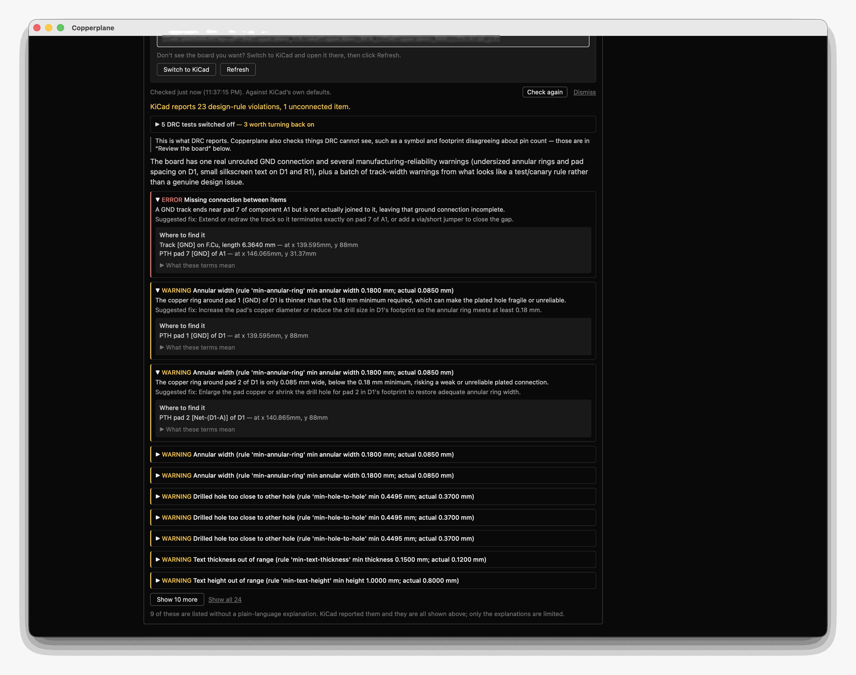
What it means: a plated through-hole pad is a ring of copper around a drilled hole. The annular ring is the copper between the hole edge and the pad edge. Yours is 0.085 mm where the board’s own rules ask for 0.100 mm. Drill placement varies by thousandths of a millimetre in manufacturing, so a ring this thin can be broken through by the drill — leaving a pad connected to nothing, on a board that looked fine in CAD.
Two — the mistake every beginner makes.
Missing connection between items: Track [GND] on F.Cu — PTH pad 7 [GND] of A1
A ground connection drawn but never finished. On a board this small you would probably catch it by eye. On a board with two hundred nets you would not.
Three — a setting, not a violation. The third finding is a suggestion: this project has the “footprint has no courtyard defined” check switched off. A courtyard is the keep-out outline marking the space a component physically occupies, and the Enclosure tab measures board-to-case fit directly from those outlines. With the check disabled, a part could be missing its courtyard and DRC would never mention it — which means the enclosure you generate later could be quietly wrong.
That one is worth dwelling on. Nothing was violated, so no checker would raise it. It is a consequence of a setting, noticed because something else in the app depends on it.
The remaining two findings are a different thing again.
Two more that KiCad never makes
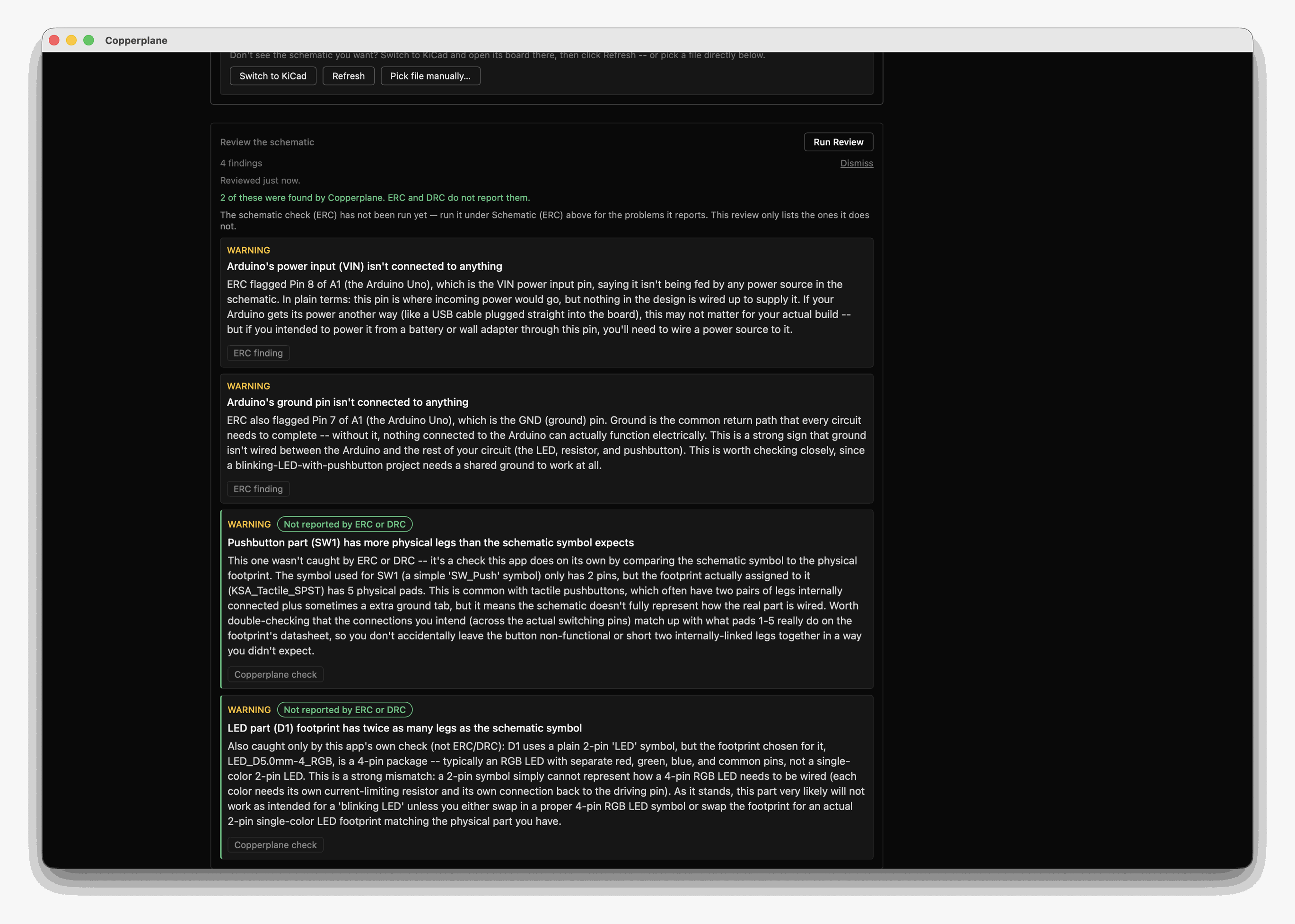
Section titled “Two more that KiCad never makes”The last two findings on that list did not come from DRC either. Like the three on Overview, they come from comparing things KiCad is happy to let disagree:
D1’s symbol and footprint disagree about how many pins this part has. The symbol
Device:LEDhas 2; the footprintLED_THT:LED_D5.0mm-4_RGBhas 4 numbered pads.
SW1’s symbol and footprint disagree about how many pins this part has. The symbol
Switch:SW_Pushhas 2; the footprintButton_Switch_THT:KSA_Tactile_SPSThas 5 numbered pads.
D1 is the one that matters. The symbol is a plain two-pin LED; the footprint is a four-pin RGB LED. Two pins driving a four-pin part: pads 3 and 4 have no net at all, and there is a single resistor where an RGB LED wants three, one per colour channel. It was never going to work.
SW1 is milder, and worth understanding for that reason. A tactile switch has four legs, internally paired, plus a shield pin. Two legs are wired and the rest sit in holes connected to nothing. It will probably work. The app does not tell you which of the two is fatal, because nothing it can measure says so — it tells you the counts disagree and lets the explanation, and you, take it from there.
Neither is a rule violation. ERC does not catch them. DRC does not report
them. Even --schematic-parity, KiCad’s own comparison of a board against its
schematic, reports zero issues on this project. There is nothing in the
toolchain that says a two-pin symbol on a four-pad footprint is a problem,
because in KiCad’s terms it isn’t one — it is a part described perfectly
consistently that happens not to exist.
That is the gap this tool exists for. A checker tells you which rules you broke. Understanding what you actually built is a different question, and it is the one that costs you a board order.
Five things on this board fall into that gap — R1’s placeholder, the 5V rail on
VIN, the two pin-count mismatches, and the LED resistor that was right all
along. None is an ERC or DRC violation. All five are things you would want
someone to mention before you spent forty dollars and a fortnight finding out.
Check the schematic
Section titled “Check the schematic”Run the schematic check. Two errors, both the same kind:
ERROR power_pin_not_driven — Input Power pin not driven by any Output Power pinsERROR power_pin_not_driven — Input Power pin not driven by any Output Power pinsThis is the single most confusing error in KiCad for anyone starting out, because the board is fine. The 5 V rail really does come from the Arduino.
KiCad cannot tell the difference between “power arrives here from off the sheet” and “you forgot to connect this”. Both look identical to it: a power input with no power output feeding it. So it asks you to say which, and a PWR_FLAG is how you say it — a symbol whose entire job is to tell ERC “power genuinely enters the design at this point, stop asking”.
The project ships without them so the check has something real to report. To fix
it the way you would on your own board: in KiCad, place a PWR_FLAG on the +5V
net and another on GND, save, and run the check again. Both errors go.
That is the whole lesson. The error was never about a broken circuit — it was KiCad asking a question, and the fix is answering it.
Fit an enclosure
Section titled “Fit an enclosure”Open the Enclosure tab.
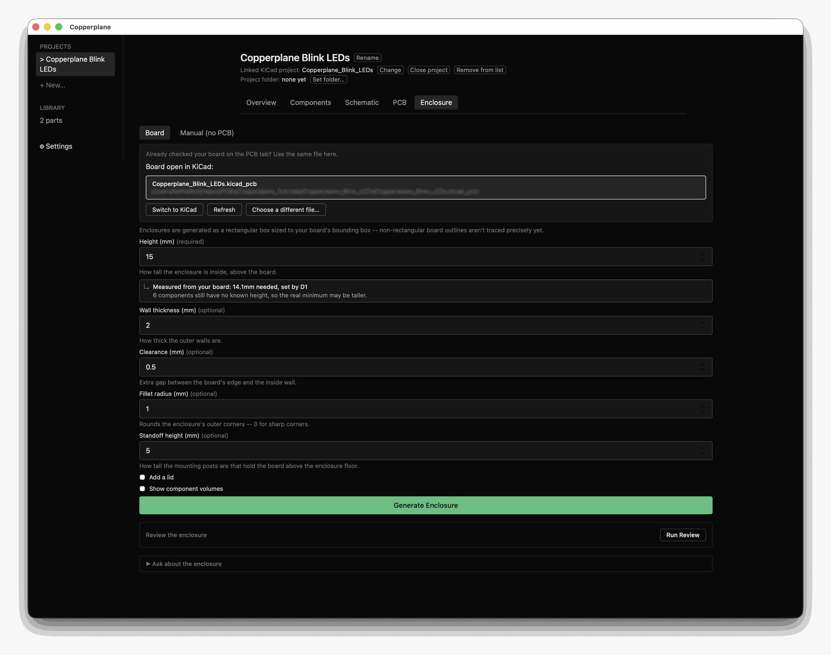
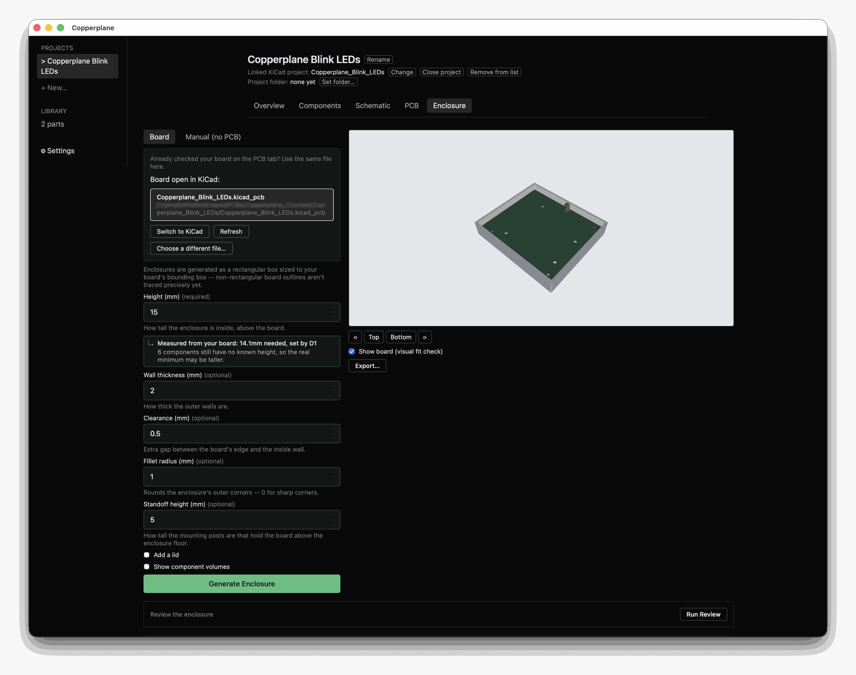
The height field is pre-filled with the 14.1 mm from earlier, and repeats the caveat: six components have no measurable height, so the real minimum may be taller. Generate, and you get a box sized to your actual board outline with the PCB seated inside it for a visual fit check.
The mounting holes are the reason this is worth doing before you order anything.
What you have learned
Section titled “What you have learned”Seven real errors between the board and the schematic, five more things that no rule checker reports, one of which was the board being right — and an enclosure that fits.
More usefully, two habits. A way of reading check output that does not depend on already knowing what an annular ring is. And the difference between “this breaks a rule” and “this will not do what you think”, which is the question that actually costs you a board order.
Everything on Overview happened without you asking. If you would rather it did not, the guided path is a toggle — off, it answers when asked and volunteers nothing. Nothing is hidden either way, and what it notices covers the rest.
Take the same pass over a board of your own. If something goes wrong — and on Windows or Linux especially, it might — tell us what happened.